When NASA’s Near Space Network set out to fly a magneto-electric dipole antenna on a high-altitude balloon, the schedule was aggressive: design, build, and launch in three months. To hit that mark, the Goddard 3D-Printing-of-Electronics team leaned on a BotFactory SV2 desktop printer for early layout and materials work—turning digital designs into test coupons in hours instead of weeks.
What NASA Needed
| Project Goal | Development Obstacle | SV2 advantage |
| Low-cost, flight-ready antenna | External PCB/ceramic runs add weeks | Desktop printing slashes turnaround |
| Custom trace geometry & substrate spacing | Multiple vendor spin | Multi-material prints from one system |
| RF tuning before committing to ceramics | Limited lab cycle time | Print → measure → tweak on the bench |
How the SV2 Fit the Process
By bringing the entire fabrication process in-house, engineering teams can fundamentally reshape their development workflow. This approach enabled a new level of flexible iteration, where engineers could print conductive and dielectric layers directly onto lab-bench substrates and immediately check critical performance metrics like impedance and gain after every minor adjustment.
This hands-on capability is magnified by true material freedom. Leveraging an open ink platform, like that of the SV2, allowed the team at NASA to trial several different conductive formulations, methodically refining their selection before committing to a final recipe optimized for the specific application.
The most profound impact of this agility is the radical compression of the development timeline. The cycle of refinement and validation shrinks from days down to mere hours. Design updates can be printed the same afternoon they are conceived, giving RF specialists a fresh set of empirical data to inform and validate the next morning’s simulation pass, creating a powerful and rapid feedback loop between design and real-world performance.
From Lab to Ladder to 100 000 ft
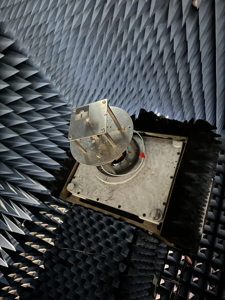
After verifying the antenna’s radiation pattern and link margin inside Goddard’s anechoic chamber, engineers took the prototype to NASA’s Columbia Scientific Balloon Facility in Texas, mounted it on a ladder, and linked it to Near Space Network satellites at multiple elevations. With ground checks complete, they launched the antenna on a weather balloon that rose to roughly 100 000 ft; telemetry stayed solid throughout the ascent, and the hardware was retrieved intact for post-flight inspection. The seamless progression from lab bench to ladder to near-space confirmed that SV2-enabled rapid prototyping can deliver high-performance flight hardware without the usual cost or schedule penalties.
Looking Ahead
We’re proud that the SV2 played a supporting role in this demonstration and excited to see additive electronics accelerate future NASA missions—whether on balloons, CubeSats, or deep-space probes. We look forward to continue supporting NASA in their chalenging, but incredibly important goals.
Read the official NASA article here
References
NASA. “NASA 3D-Printed Antenna Takes Additive Manufacturing to New Heights.” NASA Technology & Manufacturing, 28 Mar 2025. https://www.nasa.gov/technology/manufacturing-materials-3-d-printing/nasa-3d-printed-antenna-takes-additive-manufacturing-to-new-heights/