Introduction
The domain of printed electronics is undergoing a swift transformation, with substantial advancements anticipated for 2024 and 2025. This article delves into the latest research and development trends in this field, emphasizing the pivotal role of rapid prototyping and small-scale manufacturing. According to Expert Market Research, the printed electronics market, valued at USD 12.63 billion in 2023, is projected to skyrocket to USD 62.32 billion by 2032, indicating a compound annual growth rate of 19.5%. This impressive growth trajectory underscores the escalating importance and vast potential of printed electronics across various sectors.
Advanced Materials and Technologies
The exploration of new materials such as graphene and nanomaterials is a key driver of this growth, offering improved performance and efficiency. For instance, the use of graphene-based elements has been shown to influence ink viscosity, which is crucial for efficient inkjet printing. Moreover, the emergence of organic electronics signifies a significant shift towards more sustainable and eco-friendly manufacturing processes. These materials are not only cost-effective and flexible but also optically transparent and lightweight, consuming less power. This shift aligns with the global trend towards sustainable development and opens new avenues for business opportunities in electronics manufacturing.
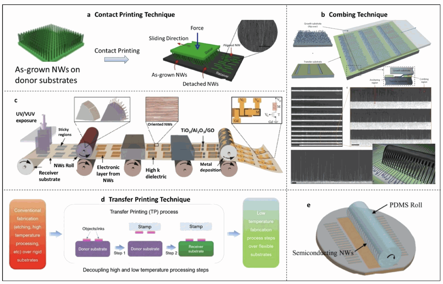
Figure: Schematic illustration for the mechanism of contact printing; A fundamental technique in printed electronics (1). The illustration shows various nanowire manipulation techniques for printed electronics; Contact printing transfers nanowires from donors to targets, combing aligns them, and multi-step transfer involves UV exposure and metal deposition for electronic components. Transfer printing and PDMS rolls enable device fabrication on flexible substrates.
In this landscape, BotFactory's SV2 PCBA Printer stands out by adopting a greener approach to PCB manufacturing, merging innovation with sustainability. The SV2 showcases material efficiency through its use of additive manufacturing techniques, significantly reducing material waste compared to traditional subtractive methods and embodying the principles of the circular economy. It's designed for energy efficiency, consuming a maximum of 400W of electric power, which dramatically lowers both operational costs and the carbon footprint associated with manufacturing electronic circuits. The printer's ability to work with a diverse array of substrates — including eco-friendly materials like glass, plastics, paper, cardboard, and wood composites, as well as dissolvable substrates made from sugarcane — enhances manufacturing flexibility while contributing to sustainability. Furthermore, the SV2 uses inks that are safer and more environmentally friendly than the hazardous acids used in traditional PCB manufacturing, eliminating the need for etchants and reducing chemical waste. It also utilizes low-temperature, lead-free solder paste, making it safer for desktop environments. Additionally, the SV2 includes components such as the component reel and tray made from recycled and repurposed filaments, showcasing a commitment to minimizing waste and supporting sustainable component sourcing. This innovative approach extends to on-demand production capabilities, which prevent overproduction and waste, making the SV2 an ideal solution for small-scale and specialized projects.
BotFactory's commitment to merging technological innovation with environmental stewardship positions the SV2 as a leading example of sustainable practices in the electronics manufacturing industry. For more detailed information on BotFactory's SV2 and its approach to greener PCB manufacturing, click here to read the full blog.
Rapid Prototyping and Small-Scale Manufacturing
Rapid prototyping and small-scale manufacturing play a central role in the evolution of printed electronics. The use of 3D printing for the creation of electronic devices with conductive features has proven particularly useful for developing Internet of Things (IoT) projects. This innovative process relies on both local deposition and local curing, making electronic parts more affordable and reducing waste of materials.

Diagram 2 illustrates the principles of screen printing and roll-to-roll fabrication used in the production of printed circuit boards (PCBs). The screen printing stages (A and B) involve a squeegee pressing ink through a mesh to form a pattern on a substrate. The roll-to-roll method (C) shows the substrate being unwound, printed, and processed through drying, sintering, and curing before being rewound. The final image (D) presents a flexible PCB, highlighting its layered structure with conductive and insulating materials, and electronic components affixed with solder paste, exemplifying the complete screen printing process in PCB creation (2).
In a comprehensive discussion, Carlos, the CEO of BotFactory, elaborated on the company’s pioneering efforts in utilizing 3D printed PCBs for small volume manufacturing and the strategic importance of additively manufactured PCBs in rapid prototyping and small-scale manufacturing. Carlos highlighted BotFactory's dedication to revolutionizing the efficiency and sustainability of these processes, significantly accelerating the pace at which prototypes are developed and small batches of electronic devices are produced. Moreover, he touched upon the intriguing potential of manufacturing in space, emphasizing how BotFactory's innovative approaches could play a crucial role in future extraterrestrial projects. This forward-thinking vision underscores BotFactory's commitment to pushing the boundaries of current manufacturing capabilities, demonstrating its pivotal role in shaping the future of electronics production both on Earth and beyond. For a deeper insight into Carlos's discussion on these transformative topics, watch the video here.
The Future of Printed Electronics
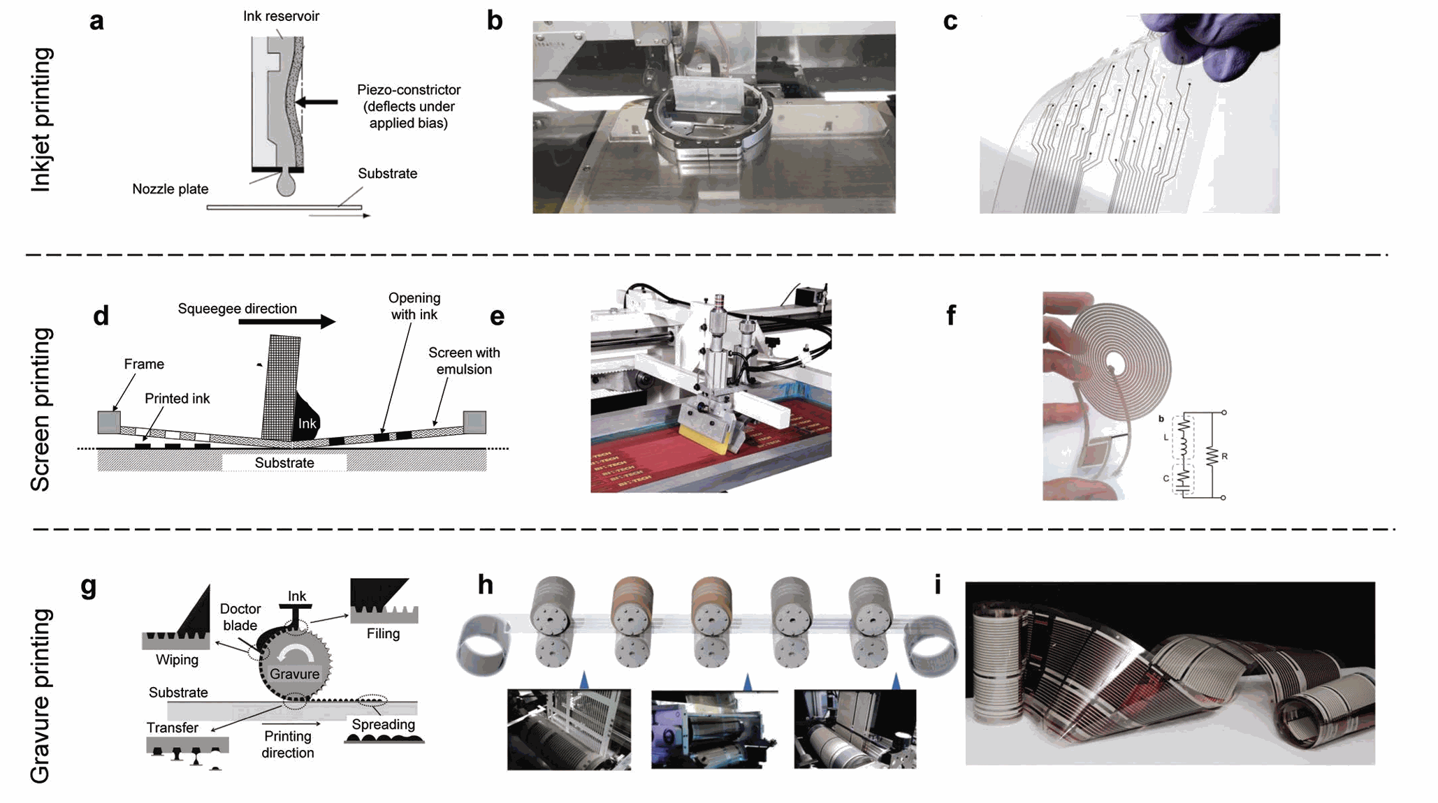
The future of printed electronics is promising, with the market expected to register a CAGR of 18.2% during the forecast period. The explosive growth of smart wearable devices, based on a new wave of digital materials, is set to augment market growth. Additionally, the increasing penetration of IoT is providing several growth opportunities, widening the scope of printed electronics applications across the sector. The images depict a series of printing and nanowire manipulation techniques essential for printed electronics manufacturing. Inkjet printing uses a piezo-constrictor to eject ink droplets onto a substrate, creating precise electronic circuits. Screen printing involves a squeegee pressing ink through a mesh screen onto a substrate, suitable for pattern creation on various materials. Gravure printing fills engraved cells with ink, wiped them clean, and then transferred them to the substrate, ideal for intricate, flexible circuits. Nanowire techniques include contact printing for pattern transfer, combing for alignment, multi-step transfer for component fabrication, transfer printing for temperature-sensitive substrates, and PDMS roll for flexible device creation (3).
Conclusion
As the printed electronics market propels forward, the demand for wearable devices, flexible displays, and the integration of IoT across various industries is bound to reach the target mentioned. The market's expansion is also driven by the advancements in rapid prototyping technologies, which are essential for the efficient production of these electronics. BotFactory is strategically positioned to leverage these industry trends with its SV2 PCBA printer, which aligns with the shift towards more agile and eco-conscious manufacturing practices. The SV2's capabilities in printing multilayer circuits and its integration of pick-and-place components cater to the growing need for rapid development cycles in printed electronics. The table below provides a summary of quantitative overview of the market's direction, highlighting the potential for BotFactory to capitalize on these advancements:
| Year | Market Size | CAGR | Key Drivers |
| 2023 | 13.59 | - | Wearable tech, IoT |
| 2024 | 15.6 | 18.2% | Flexible displays, organic materials |
| 2025 | - | - | Rapid prototyping, 3D printing |
| 2031 | 56.69 | 17.8% | Sustainable manufacturing, advanced materials |
BotFactory's SV2 PCBA printer is well-equipped to meet the evolving demands of this burgeoning market, offering a solution that is both innovative and sustainable. As the industry continues to grow, BotFactory remains committed to providing state-of-the-art solutions that enable the rapid and eco-friendly development of printed electronics.